Skip to main content Skip to footer
Home
User manuals

Main navigation

  • Home
  • Enterprise for Engineers
    • Program overview
      • Getting started
      • Product browser
      • Recent activity
      • Viewer tab
        • Product viewer
      • Specifications tab
        • Product Specifications viewer
        • Product documentation
        • Product buildup viewer
        • PCBA Components
        • Product sharing
      • Quotation
      • History
      • Shopping Cart
    • File menu
    • Show menu
      • Find product
      • View mode
    • Products menu
    • Operations menu
      • Import PCB
      • Panelize PCB
      • Create Stencil
      • Add Masks to PCB
      • Assembly Data Manager
      • Solder Pallet Designer
      • Depanelize PCB
      • Test Fixture
      • Test Fixture (legacy)
      • Connector chooser
      • Import 3D Mechanical Part
      • Order History
    • Configuration menu
      • Partner manager
      • User details
      • User manager
      • Options
      • Move ME to new PC
    • What's new
    • Release notes
  • Enterprise for Purchasers
    • Activity Overview
    • Product details
    • Search for product
    • Additional Operations
      • Partner manager
      • User profile
      • User manager
      • Options
  • Macaos Gallery
    • Product Browser
      • Product Explorer
      • Simple PCB Editor
      • Exporting product data to Gerber
      • Searching for products
      • MIF File history
      • Icon bar
      • Product info
    • Operations
      • Standard operations
        • Import PCB
        • Panelize PCB
        • Create Stencil
        • Add Masks to PCB
      • EMS version operations
        • Assembly Data Manager
        • Solder Pallet Designer
        • Depanelize PCB
        • Test Fixture
    • Technical Documentation
    • Configuration
    • Gallery PreCAM
      • Configuration options
      • Quotation module
        • Quotations
        • Calculated prices
        • Adjusting prices
        • Quotation
      • Quotation archive
        • Folders
      • Price Editor module
      • Price list editor
        • Price element editor
        • Selector editor
        • Curve editor
        • Price list wizard
      • Sales office settings
      • Holidays
      • About prices
        • Factory price
        • Retail price
        • How is a price calculated?
      • Reference
        • Price list
        • Price element
        • Curve function
        • Parameters
      • Example: Creating the Demo price list
        • Using the price list wizard
        • Refining the price list
        • Retail price
    • What's new
    • Release notes
  • Subsystem Manuals
    • Product editor Modules
      • Assembly Data Manager (ADM)
      • Assembly Masks
      • Depanelization
      • Import PCB
      • Mechanical Parts
      • Panelization
      • Solder Pallet
      • Solder Paste Stencils
      • SPRINT Test Fixtures
      • Test Fixtures (Legacy)
    • Product display modules
      • PCBA Components
      • Product Buildup Viewer
      • Product History
      • Product Specifications Viewer
      • Product Viewer
    • Other Modules
      • Connector Chooser
      • Order History
      • Partner Manager
      • Product sharing
      • Quotation
      • Search
      • Shopping Cart
      • User Details
      • User Manager
  • Additional info
    • Release notes
      • What's new in ME for Engineers
      • What's new in ME for Purchasers
      • What's new in Gallery
      • What's new in Convergence
      • ME for Engineers release notes
      • ME for Purchasers release notes
      • Gallery release notes
      • Convergence release notes
      • Perception release notes
    • Gerber file generation tips
      • Using KiCad
      • Using Eagle
      • Using CADint
      • From other systems
    • Performance Classes
    • Solder paste stencil ratios
    • Surface finishes
    • Via types
    • Panelization scripts
  • Contact
  • Back to Macaos website

Component footprints

Home plate padsComponent footprintsIt is possible to modify stencil openings by component footprint. Non-symmetric openings (such as home plate or bow tie shapes) are automatically oriented correctly for pads on each side of the component. This operation can be performed on a single component or on multiple components with the same footprint.

Note: Component footprint editing is only supported for PCBs where test pad data is available. If test pad data (in IPC-D-356 format) was not imported when the product was created, it may be added to the product in the Assembly Data Manager.

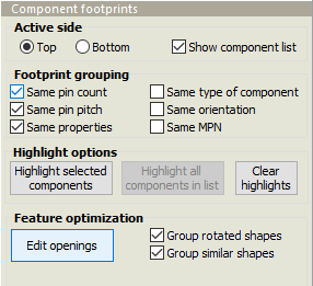
When an active side is chosen, the paste mask openings are mapped to the test pad data, in order to determine which openings belong to the same component. Based on this, a list of components (grouped by the selected grouping parameters) is displayed.

Select one or more components in a group and click on the Highlight selected components button to zoom to and highlight the components. Then click on the Edit openings button to open the Split or edit stencil openings dialog box. Clicking on the Replace openings button in the dialog box copies the new opening parameters to all openings of all selected components. If the footprint has multiple opening sizes/shapes (or either of the Group options is unchecked) then use the Prev/Next buttons to edit each of the different shapes in the footprint. Note: You can double-click on a group to zoom, highlight and open the editor in a single operation.

Footprint iconsEach component in the list has a blue icon, which indicates the type of footprint. Once a component has been edited, it gets a pink icon which indicates the opening shape. Use the Hide edited components check box to exclude components from the list after they have been edited.

If desired, you can locate components by designator with the filter text at the bottom of the list. When the list is filtered, then the Highlight all components in list button will zoom to and highlight all of the components in the filtered list.

Note: Do not confuse test pads with test points or test pins.

  • Test pads are the locations for bare-board testing of the PCB during manufacture, which are extracted from an IPC-D-356 file to the Test pads layers.
  • Test points are specific pads or pins on the PCBA which would be used for in-circuit testing. For each test point, a “component” (with the Test point component class) should be added to the appropriate component layer. Ideally, test points (with TPxx designators) should be included in Pick and Place data, but they may also be created manually.
  • Test pins are the pins in a test fixture which will make contact with the PCBA during in-circuit testing.

Book traversal links for Component footprints

  • ‹ Transfer objects from other layers
  • Up
  • Stencil frames ›

Macaos Software AS
Sanddalsringen 5b
N-5225 Nesttun
Norway

Download gerber specification
ODB++ partner
IPC member

Footer menu

  • Contact
  • Privacy policy
Powered by Drupal

Copyright © 2025 Macaos Software AS - All rights reserved