Contour tools
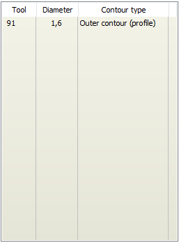 The Contour tab lists the cutting tools used for milling contours and slots. The diameter of a contour tool is initially specified when importing the board product. The tool diameter determines the width of plated and unplated slots. For inner and outer contours, it determines the radius of inner corners, and must be small enough to fit into any notches in the contour. For outer contours, it also determines the minimum instance spacing when panelizing.
Cutting tools are listed with a tool number, diameter (mm), and contour type. The tool number determines the contour type:
60-69: Plated slot
70-79: Unplated slot
80-89: Inner contour (cutout)
90-94: Outer contour (profile)
95: Scoring
Diameters must be between 0.4 and 5.0 mm. There may only be one outer contour (even though there are five possible tool numbers). Any valid tool number may have any valid diameter.
Viewing contours and slots: Double-click a tool to highlight the slots or contour outlines which use the tool. Note: Slots are normally drawn to hide all material removed by the slot, which also hides the highlighted features. Therefore the Route MIF layer is automatically turned off when double-clicking a contour tool.
Right-click on a cutting tool to select the following operations:
Change diameter: Enter the new diameter (in mm). This will affect all slots which use the selected tool. Note: This operation is not available for scoring tools.
Toggle plating: Toggle a slot between plated and unplated. Note: This operation is only available for slot (60-79) tools.
Drill tools
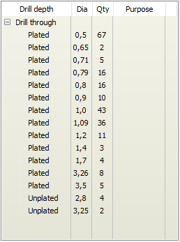 The Drill tab lists all drill depths (MIF layers) and their drill tools (shapes). For each tool, the plating state, diameter (in mm), hole (feature) quantity, and hole purpose (if any) is listed.
Double-click a tool to highlight features which use the tool. Use the Show highlight check box to toggle highlight visibility.
Right-click on a drill tool to select the following operations:
Change diameter: Enter a new diameter (in mm) to modify the tool diameter.
Toggle plating: Change the plating state from plated to unplated, or vice versa.
Mark holes as: Select a hole style from the submenu. In addition to via protection types, holes may be marked as press-fit or countersinked. To change the hole style for all tools using a hole style, use the Reassign layer operation in the Layers list.
Note: These operations affect all holes which use the selected tool.
Right-click on a drill MIF layer to select the following operations:
Reassign layer: Select a new drill extent. If selecting blind or buried, you must also specify the blind depth or start/stop copper layers.
Replace layer: In some cases, it may be desirable to update a drill MIF layer with a modified Gerber file. After selecting the replacement Gerber file, the old (red) and new (cyan) MIF layers are shown in the viewer. Accept or abandon replacing the MIF layer. Note: The replacement Gerber image must have exactly the same outer dimensions as the MIF layer being replaced.
Delete layer: Remove the selected MIF layer from the product.
Layers
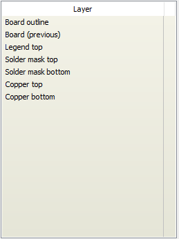 The Layer tab lists all MIF layers in the product except mechanical (contour and drill) layers.
Right-click on a MIF layer to select the following operations:
Reassign layer, and select the new MIF layer (or select Change to positive or Change to negative to change the layer polarity). If the selected MIF layer already exists, the two layers will be swapped. To change the hole style for a single drill tool, use the Reassign layer operation in the Drill list. Note: This operation is only valid on a copper or via protection MIF layer.
Replace layer: In some cases, it may be desirable to update a single MIF layer with a modified Gerber file. After selecting the replacement Gerber file, the old (red) and new (cyan) layers are shown in the viewer. Accept or abandon replacing the MIF layer. Note: The replacement Gerber image must have exactly the same outer dimensions as the MIF layer being replaced.
Delete layer: Remove the selected MIF layer from the product.
Details
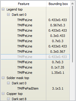
The Details operation allows viewing objects in the MIF data structure. Each layer in the board is made up of one or more sets. Each set contains one or more features, and specifies whether the features draw (dark) or erase (clear) the graphic result. Each feature is a graphical object (line, arc, pad, polygon, etc.) at a specific location. Most features have a shape, which is the pen width for a line or arc, or the appearance of a pad.
Selected features on visible layers may be inspected, and optionally modified as follows:
Press the Details button, so that it is active (down).
Left-click and draw a selection rectangle. All selected features on visible layers will be listed, grouped by MIF layer and set.
Double-click on a feature to highlight and zoom to the feature.
Right-click on a feature to highlight all features which use the same shape as the feature.
Click on a MIF layer, set, or feature to load it into the Object Properties module. If a feature is selected, separate property lists are shown for the feature and for its shape.
Note: Editing shape properties will affect all features which use the shape.
Press the Edit button to enable editing. Press the Save button to save changes, or the Reset button to restore the settings. While in Edit mode, click on a property value to modify the value. For editable properties, an in-place or popup editor will open so that the new value may be entered. Some properties may not be modified; in which case nothing happens when clicking on the value.
Note: Care should be taken when modifying geometric properties, such coordinates, rotation, etc. Careless changes could make the entire product invalid.
Press the Details button again to exit Details mode.
Use the Show highlight check box to toggle highlight visibility.
Converting composite shapes
Right-click on a feature which uses a composite shape, and choose Convert to rounded rectangle to change the type of shape. If the composite shape was a collection of circles and rectangles making up a rounded rectangle, then resulting RoundRect shape should have the same dimensions. If not, then you may need to edit the shape properties to achieve the desired result. When converting, the user may choose between converting for all features which use the shape, or only for the selected feature.
Note: Component features may not be edited; the ADM should be used for modifying components.
Crop
Press the Crop button to delete all features on visible MIF layers, which are not completely or partially inside the outer contour of the product. Note: No features are deleted from layers which are not visible at the time the button is pressed.
Delete
Selected features on visible MIF layers may be deleted as follows:
Press the Delete button, so that it is active (down).
Left-click and draw a selection rectangle. All features on visible MIF layers which are completely or partially within the rectangle are deleted.
Press the Delete button again to exit Delete mode.
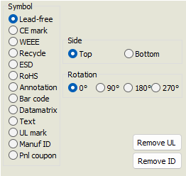 Symbol
While the Symbol button is active (down), it is possible to add symbols to the product, as follows:
Select the desired symbol type.
Depending on the symbol type, select the desired MIF layer, side, and rotation. For bar codes or text, specify the text string. For text, specify the font height.
For bar codes, text, Manuf ID or Pnl coupon, click at the desired location. For other symbol types, draw a selection rectangle defining the symbol size and location.
See the Symbols page of the Import module for more information about available symbols.
DRC
The DRC processor automatically runs a number of checks on the product. The DRC report always reflects the current state of the product (in the PCB editor), so any changes which have been made (within the PCB Editor) are included in the report.
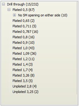 Generating a CAM report analyzes all holes on all drill layers, looking for the following anomalies:
Tool/hole plating mismatch: Holes marked as plated using tools marked as unplated (or vice versa).
No pads found on either side: Plated tool holes without any copper pads larger than the hole diameter, on either the start or stop layer of the drill hole.
Pad on only one side: Plated tool holes with a copper pad larger than the hole diameter, on either the start or stop layer of the drill hole, but not both.
Has pads on one or both sides: Unplated tool holes with copper pads on either the start or stop layer of the drill hole, or both.
No SM opening on either side: Holes without any solder mask opening on either side. For blind vias, only the outer layer is checked. Buried vias are not checked.
SM opening on only one side: Holes with solder mask opening on only one side. Applies only to through holes.
SM opening/via fill mismatch: Holes where the presence or absence of solder mask openings is inconsistent with the via filling type.
Hole property mismatch: One or more of the following:
Tool purpose (.AperFunction) does not match co-located pad on via filling type layer
Tool purpose is specified, but no co-located pad found on via filling type layer
Co-located pads found on multiple via filling type layers
The list is sorted by layer, tool, and anomaly (if any are found). All drill layers and tools are listed. Only those holes which have anomalies are listed.
Note: The hole analysis only looks for Pad features (flashes) on the copper, solder mask and via filling type layers. It is unable to recognize drawn objects or ground planes as being present at the same location as the hole. It may, therefore, report anomalies which are not actually a problem.
Highlight and zoom: Double-click on a tool, anomaly, or hole in the list to highlight and zoom to the hole(s). Use the Show highlight check box to toggle highlight visibility.
Corrective operations: Various operations are available to correct hole anomalies. Right-click on a row in the list to make corrections. Selecting an anomaly will act on all holes with that anomaly. Selecting a single hole will act on only the selected hole. Some operations may be carried out on the tool rather than on holes.
Toggle tool/hole plating: Change the plating of the selected tool or hole(s).
Add copper pads: Add copper pads (with user-specified diameter) to selected hole(s).
Remove copper pads: Remove all pads on start/stop layers at same location as hole(s).
Add solder mask openings: Add openings (with user-specified diameter) to selected hole(s).
Remove solder mask openings: Remove openings on outer layers at same location as hole(s).
Change tool/hole purpose: Reassign the via filling type of the selected tool or hole(s).
Split tool by purpose: Split a tool with mixed purposes into separate tools for each purpose.
Note: Hole analysis can be a time-consuming operation, if there are many holes on many depth-extent layers. For this reason, the holes list is not automatically updated after each corrective operation. To update the list after making corrections, press the DRC button or right-click and choose Refresh list to run the analysis and view an updated DRC report.