- Select pallet style. Upon starting the pallet designer module, select the Selective wave solder pallet style.
- Specify board placement. The board is placed in the center of the pallet with top side up. If desired, you may rotate or flip the board by clicking on the appropriate button in the Placement tool bar.
Specify pallet properties. Specify the product name, article and description. Adjust the pallet dimensions, if necessary. Select a pallet material and thickness. Check that the PCB thickness is correct. If the board does not require a lead-free soldering process, remove the Pb-Free check mark. Specify pocket depths for solder-side component pockets.
Place board fasteners. Specify the length (from pivot-point to end) of the fasteners, and how much they should overlap the board edges. Then click on the Place button (so that it is down). Click and drag the circle to the desired location, then release the mouse button to place a fastener. Repeat as necessary.
If you need to delete a fastener, click on the Delete button (so that it is down). Draw a selection rectangle around the entire fastener and circle that you wish to delete.
Specify openings in the pallet. Select Pallet opening as the active layer. Select one of the three drawing modes to draw the boundary of the opening.
- Draw rectangle: Click at one corner of the rectangle, then drag the mouse pointer to the opposite corner and release.
- Draw outline: Click at one vertex of the outline, drag the mouse pointer to the next vertex and release the mouse button. Click and drag to each additional vertex of the outline. All edges automatically snap to orthogonal or diagonal. To close the outline, press the F9, Space or Return key. To abort creation of the outline, press the Esc key.
- Draw orthogonal outline: Use the same technique as for drawing an outline. All edges automatically snap to orthogonal.
To delete an outline, click on the Delete button (so that it is down). Draw a selection rectangle around the entire outline that you wish to delete.
 Keep the following rules in mind while defining pallet openings:
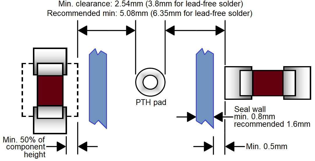
- Minimum clearance between the edges of pallet openings and PTH pads is 1.24 mm for PbSn soldering or 2.5 mm for lead-free soldering.
- Aspect ratio guidelines must be followed.
Note: When working with a (single-product) panel which has been created with the Macaos panelization module, the first board in the panel is highlighted with a yellow rectangle. Openings and pockets specified within this rectangle will automatically be copied to all other boards in the panel.
Specify pockets. Repeat the process of step 5 for component pockets, as necessary.
 Keep the following clearance rules in mind while defining component pockets:
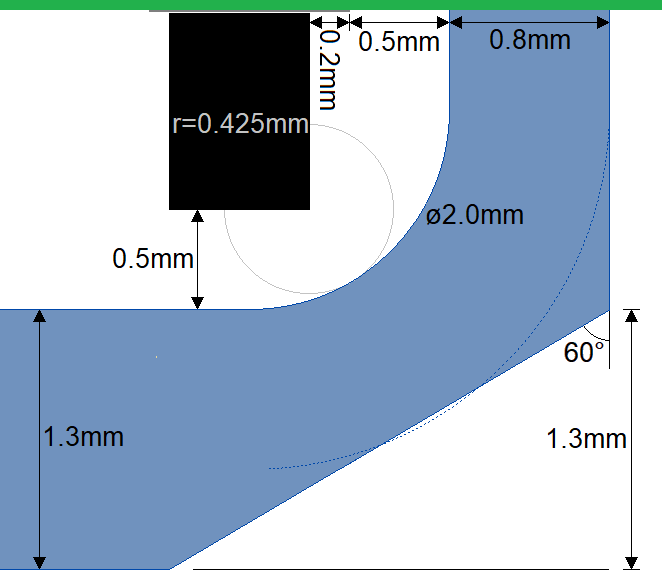
- Minimum 0.8 mm clearance between pocket edges and the edges of pallet openings.
- Minimum 0.5 mm clearance between component and pocket floor.
- Minimum 0.5 mm clearance between pocket edge and component pad, when component is perpendicular to pocket edge. When component is parallel to pocket edge, the minimum clearance is increased by 50% of the component height.
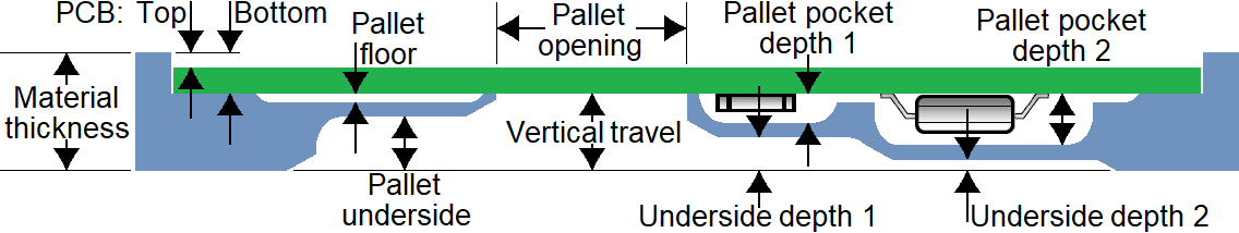
Note: The pallet floor (0.5mm clearance under the PCB) is defined automatically based on the PCB outline and the pallet openings. Likewise, pressure relief regions (on the bottom side) are defined automatically based on the pallet openings and component pockets.
Note: If a pocket is drawn too close to an opening, it will automatically be clipped to give a 0.8 mm clearance between the pocket and the opening.
- Generate a milling file. If desired, a milling file may be generated. The milling file(s) may be used to make the pallet with your own milling machine. Click on the Save button to save the milling file in G-Code format. After specifying a file name, the Milling program setup dialog box is used to specify the necessary parameters to generate an output file with the correct coordinates and operating commands for the target milling machine. See also our solder pallet milling guidelines.
- Publish or save the pallet product. Use the Publish (Macaos Enterprise) or Save (Macaos Gallery) button to save the product. It may then be reopened for modification or to generate a milling file. It is also possible to purchase a finished pallet product (with stiffeners and fasteners).
User manuals
Creating a selective wave solder pallet
Elprint AS
Sanddalsringen 5b
N-5225 Nesttun
Norway


Copyright © 2026 Elprint AS - All rights reserved