With the Simple PCB Editor, it is possible to make certain adjustments to a PCB product. You can:
- Change the diameter or slot plating of a contour tool
- Change the diameter, plating, or purpose of a drill tool
- Change the extent (depth) of a drill layer
- Reassign a copper layer
- Change the polarity of a copper layer
- Change the via protection, press-fit, or countersink style of a hole style layer
- Replace a layer with the contents of a Gerber file
- Crop (delete) all graphic objects outside of the board’s outer contour
- Delete selected graphic objects
- Add symbols to the legend or solder mask layers
- View, and in some cases modify, object properties in the PCB's data structure
The Edit Board menu item in the product browser opens the selected product in the Simple PCB Editor. With this editor, it is possible to modify the graphic objects in the product's MIF data structure.
The Simple PCB Editor consists of a left column for editing operations, and a product viewer on the right.
Please note: The Simple PCB Editor is not intended to be a substitute for an Electronic CAD system. It is primarily intended for minor adjustments to Macaos Gallery products. Editing a PCB must be done with care. It is possible to make changes which could render the entire board invalid. The user is responsible for any data loss which may occur through the use of the Simple PCB Editor.
Simple PCB Editor operations
Save: Save the product MIF data
MIF history: Open's the MIF file history viewer
Change log: Show a report of changes since the last Save operation.
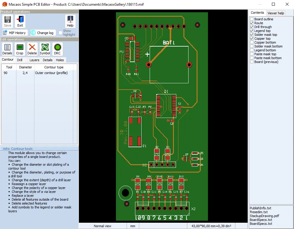
Contour: View and modify contour tool properties
Drill: View and modify drill tool properties
Layers: View and modify non-mechanical MIF layers
Details: View and edit feature and shape properties
Crop : Delete features which extend outside of the outer contour
Delete: Delete selected features
Symbol: Add a symbol to the product
DRC: Generate a DRC report for the product.
Features may be highlighted to view more easily locate and view the features in the MIF viewer. Highlighted features are shown in white. It may be useful to turn off the Legend MIF layer(s) in order to make the highlighted features more visible. Use the Show highlight check box to toggle visibility of the currently highlighted features.
The editor maintains a log of all MIF edit operations. This log may be viewed by pressing the Change log button. The log is stored in the product’s MIF file history when the product is saved.
Product properties
Product properties which affect the product type (flex/mbb/etc.) and/or layer count (stackup, layer count, flex layer count) should be modified prior to opening the Simple PCB Editor.
Most properties which can be extracted from the MIF data are automatically updated when the Simple PCB Editor saves the product. This includes all properties except:
Specifications: Solder mask, legend and cover layer colors, stackup, surface finish, flex layer count, thermal conductivity, and beveled edge parameters.
Statistics: Minimum track width and clearance, boards/pnl, and diff. boards/pnl