Skip to main content Skip to footer
Home
User manuals

Main navigation

  • Home
  • Enterprise for Engineers
    • Program overview
      • Getting started
      • Product browser
      • Recent activity
      • Viewer tab
        • Product viewer
      • Specifications tab
        • Product Specifications viewer
        • Product documentation
        • Product buildup viewer
        • PCBA Components
        • Product sharing
      • Quotation
      • History
      • Shopping Cart
    • File menu
    • Show menu
      • Find product
      • View mode
    • Products menu
    • Operations menu
      • Import PCB
      • Panelize PCB
      • Create Stencil
      • Add Masks to PCB
      • Assembly Data Manager
      • Solder Pallet Designer
      • Depanelize PCB
      • Test Fixture
      • Test Fixture (legacy)
      • Connector chooser
      • Import 3D Mechanical Part
      • Order History
    • Configuration menu
      • Partner manager
      • User details
      • User manager
      • Options
      • Move ME to new PC
    • What's new
    • Release notes
  • Enterprise for Purchasers
    • Activity Overview
    • Product details
    • Search for product
    • Additional Operations
      • Partner manager
      • User profile
      • User manager
      • Options
  • Macaos Gallery
    • Product Browser
      • Product Explorer
      • Simple PCB Editor
      • Exporting product data to Gerber
      • Searching for products
      • MIF File history
      • Icon bar
      • Product info
    • Operations
      • Standard operations
        • Import PCB
        • Panelize PCB
        • Create Stencil
        • Add Masks to PCB
      • EMS version operations
        • Assembly Data Manager
        • Solder Pallet Designer
        • Depanelize PCB
        • Test Fixture
    • Technical Documentation
    • Configuration
    • Gallery PreCAM
      • Configuration options
      • Quotation module
        • Quotations
        • Calculated prices
        • Adjusting prices
        • Quotation
      • Quotation archive
        • Folders
      • Price Editor module
      • Price list editor
        • Price element editor
        • Selector editor
        • Curve editor
        • Price list wizard
      • Sales office settings
      • Holidays
      • About prices
        • Factory price
        • Retail price
        • How is a price calculated?
      • Reference
        • Price list
        • Price element
        • Curve function
        • Parameters
      • Example: Creating the Demo price list
        • Using the price list wizard
        • Refining the price list
        • Retail price
    • What's new
    • Release notes
  • Subsystem Manuals
    • Product editor Modules
      • Assembly Data Manager (ADM)
      • Assembly Masks
      • Depanelization
      • Import PCB
      • Mechanical Parts
      • Panelization
      • Solder Pallet
      • Solder Paste Stencils
      • SPRINT Test Fixtures
      • Test Fixtures (Legacy)
    • Product display modules
      • PCBA Components
      • Product Buildup Viewer
      • Product History
      • Product Specifications Viewer
      • Product Viewer
    • Other Modules
      • Connector Chooser
      • Order History
      • Partner Manager
      • Product sharing
      • Quotation
      • Search
      • Shopping Cart
      • User Details
      • User Manager
  • Additional info
    • Release notes
      • What's new in ME for Engineers
      • What's new in ME for Purchasers
      • What's new in Gallery
      • What's new in Convergence
      • ME for Engineers release notes
      • ME for Purchasers release notes
      • Gallery release notes
      • Convergence release notes
      • Perception release notes
    • Gerber file generation tips
      • Using KiCad
      • Using Eagle
      • Using CADint
      • From other systems
    • Performance Classes
    • Solder paste stencil ratios
    • Surface finishes
    • Via types
    • Panelization scripts
  • Contact
  • Back to Macaos website

Reduced thickness (stepped) regions

Reduced thickness regionsIn some cases it may be desirable to “step” a stencil (that is, reduce the thickness of a region of a stencil), in order to better control the amount of solder paste to be applied.

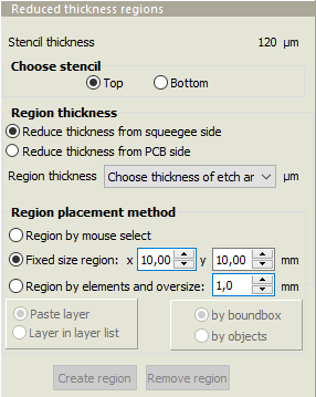
Stencil thickness is reduced in a region by etching the region until the region's thickness has been reduced to the desired thickness. This is done prior to cutting openings in the stencil.

To define reduced thickness regions, specify the side and thickness for the region, select a placement method, click on the Create region button (so that it is down) and then draw (or place) a rectangle on the stencil to define the region.

The region thickness should be defined as the desired thickness for the specified region.

Typically, etching will be done from the squeegee (top) side of the stencil, leaving a flat surface against the PCB. But in some cases, such as when there is a sticker on the PCB, it may be desirable to etch a region from the PCB (bottom) side.

There are three methods for placing a reduced thickness region:

Region by mouse select: Draw a selection rectangle on the stencil to define the region. The region boundaries must be at least 0.5mm from any stencil openings or other regions on the stencil.

Fixed size region: Specify the region dimensions and then place the rectangle where desired.

Region by elements and oversize: Specify an oversize dimension (in mm) and then draw a selection rectangle around the objects to be included in the region.

  • Paste layer: The objects will be selected from the paste mask top or bottom layer
  • Layer in layer list: The objects will be selected from the highlighted layer
  • by boundbox: The region will be created as a rectangle with a clearance of at least the specified oversize dimension from the selected objects on all sides
  • by objects: The region will be the specified oversize dimension larger than the selected objects on all size, following the shape(s) of the selected objects.

To remove a region from the stencil, click on the Remove region button (so that it is in the down position), select the region thickness and then draw a selection rectangle around any portion of the region(s) to remove. Once you have removed the regions you wish to delete, click the Remove region button again to exit delete mode.

Note: Creating reduced thickness regions will increase the cost of the stencil.

Book traversal links for Reduced thickness (stepped) regions

  • ‹ Delete objects
  • Up
  • Transfer objects from other layers ›

Macaos Software AS
Sanddalsringen 5b
N-5225 Nesttun
Norway

Download gerber specification
ODB++ partner
IPC member

Footer menu

  • Contact
  • Privacy policy
Powered by Drupal

Copyright © 2025 Macaos Software AS - All rights reserved