Skip to main content Skip to footer
Home
User manuals

Main navigation

  • Home
  • Enterprise for Engineers
    • Program overview
      • Getting started
      • Product browser
      • Recent activity
      • Viewer tab
        • Product viewer
      • Specifications tab
        • Product Specifications viewer
        • Product documentation
        • Product buildup viewer
        • PCBA Components
        • Product sharing
      • Quotation
      • History
      • Shopping Cart
    • File menu
    • Show menu
      • Find product
      • View mode
    • Products menu
    • Operations menu
      • Import PCB
      • Panelize PCB
      • Create Stencil
      • Add Masks to PCB
      • Assembly Data Manager
      • Solder Pallet Designer
      • Depanelize PCB
      • Test Fixture
      • Test Fixture (legacy)
      • Connector chooser
      • Import 3D Mechanical Part
      • Order History
    • Configuration menu
      • Partner manager
      • User details
      • User manager
      • Options
      • Move ME to new PC
    • What's new
    • Release notes
  • Enterprise for Purchasers
    • Activity Overview
    • Product details
    • Search for product
    • Additional Operations
      • Partner manager
      • User profile
      • User manager
      • Options
  • Macaos Gallery
    • Product Browser
      • Product Explorer
      • Simple PCB Editor
      • Exporting product data to Gerber
      • Searching for products
      • MIF File history
      • Icon bar
      • Product info
    • Operations
      • Standard operations
        • Import PCB
        • Panelize PCB
        • Create Stencil
        • Add Masks to PCB
      • EMS version operations
        • Assembly Data Manager
        • Solder Pallet Designer
        • Depanelize PCB
        • Test Fixture
    • Technical Documentation
    • Configuration
    • Gallery PreCAM
      • Configuration options
      • Quotation module
        • Quotations
        • Calculated prices
        • Adjusting prices
        • Quotation
      • Quotation archive
        • Folders
      • Price Editor module
      • Price list editor
        • Price element editor
        • Selector editor
        • Curve editor
        • Price list wizard
      • Sales office settings
      • Holidays
      • About prices
        • Factory price
        • Retail price
        • How is a price calculated?
      • Reference
        • Price list
        • Price element
        • Curve function
        • Parameters
      • Example: Creating the Demo price list
        • Using the price list wizard
        • Refining the price list
        • Retail price
    • What's new
    • Release notes
  • Subsystem Manuals
    • Product editor Modules
      • Assembly Data Manager (ADM)
      • Assembly Masks
      • Depanelization
      • Import PCB
      • Mechanical Parts
      • Panelization
      • Solder Pallet
      • Solder Paste Stencils
      • SPRINT Test Fixtures
      • Test Fixtures (Legacy)
    • Product display modules
      • PCBA Components
      • Product Buildup Viewer
      • Product History
      • Product Specifications Viewer
      • Product Viewer
    • Other Modules
      • Connector Chooser
      • Order History
      • Partner Manager
      • Product sharing
      • Quotation
      • Search
      • Shopping Cart
      • User Details
      • User Manager
  • Additional info
    • Release notes
      • What's new in ME for Engineers
      • What's new in ME for Purchasers
      • What's new in Gallery
      • What's new in Convergence
      • ME for Engineers release notes
      • ME for Purchasers release notes
      • Gallery release notes
      • Convergence release notes
      • Perception release notes
    • Gerber file generation tips
      • Using KiCad
      • Using Eagle
      • Using CADint
      • From other systems
    • Performance Classes
    • Solder paste stencil ratios
    • Surface finishes
    • Via types
    • Panelization scripts
  • Contact
  • Back to Macaos website

Layers

Breadcrumb

  • Home
  • Import PCB
  • Layers

Layers
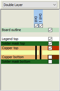
A printed circuit board is made up of several “layers”. These include copper layers, mask and legend layers, drill files and more. Each layer is described by one (or sometimes two) image files, and normally a file describes only one layer. The Layer overview shows the filenames and layer names of the board. The check boxes for each layer may be used to view or hide the layer in the graphic display. The rectangle to the right of the check box shows the color used to display the layer in the Graphic Display. You can right-click on this rectangle to change the color.

The Route layer is automatically generated by adding contour objects (in the Contour pane).

The controls at the top of the Layer Overview may be used to specify the number of copper layers on the board. This is automatically increased if you link additional layers in the Files pane. However, if you want to reduce the number of copper layers, you must do so here.

For single layer boards, it is not possible to link a soldermask file to the non-copper side of the board. In the Board Specifications pane, the soldermask color for the non-copper side will be set to None. Changing this to another color will indicate that the board should have soldermask on the non-copper side.

You may right-click on the layer overview to quickly show only top layers, only bottom layers, all layers or no layers.

Book traversal links for Layers

  • ‹ Creating a board product
  • Up
  • Linking files ›

Macaos Software AS
Sanddalsringen 5b
N-5225 Nesttun
Norway

Download gerber specification
ODB++ partner
IPC member

Footer menu

  • Contact
  • Privacy policy
Powered by Drupal

Copyright © 2025 Macaos Software AS - All rights reserved