The product specifications viewer lists product specifications in one or more tabs, depending on the product type.
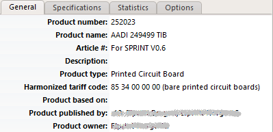 General (all product types)
- Product number: Macaos product number
- Product name: Customer's product name
- Article number: Customer's article number
- Description: Customer's product description
- Harmonized tariff code: Import tariff code for product
- Based on product number: Macaos product number from which this product is derived.
- Product published by: Macaos license number, user name, and company name of person who created the product.
- Product owner: Company name of the partner which owns the product, if product is shared to your company.
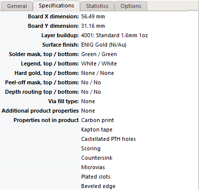 Specifications (PCB products)
- Board X dimension (mm): Maximum width of the PCB.
- Board Y dimension (mm): Maximum height of the PCB.
- Layer buildup: The name or description of the layer buildup.
- Surface finish: This is usually an extra cost feature for finishes other than lead-free HASL.
- Solder mask color, top/bottom side
- Legend (silkscreen) color, top/bottom side: Also called silkscreen or notation.
- Hard gold area, top/bottom side (cm²): Also called electrolytic gold. This is usually an extra cost feature.
- Peel-off mask, top/bottom side (yes|no): This is usually an extra cost feature.
- Depth routing from top/bottom side (yes|no): This is usually an extra cost feature.
- [If flex or rigid-flex] Flex stiffener, top/bottom side (yes|no): This is usually an extra cost feature.
- [If flex or rigid-flex] Cover layer color, top/bottom side: This is usually an extra cost feature.
- [If rigid-flex] Flexible layer count
- [If metal-based board] Thermal conductivity (W/m-K)
- IPC-4761 Via filling type: This is usually an extra cost feature.
The following product properties are either listed under Additional product properties (if present) or Properties not in product (if not present.
- Carbon print: The PCB has carbon print. This is usually an extra cost feature.
- Kapton tape: The PCB requires Kapton tape. This is usually an extra cost feature.
- Castellated PTH holes: Plated holes that extend outside of the board edge. Also called half-moon holes or plated half-holes. This is usually an extra cost feature.
- Scoring: The PCB has scoring. Also called V-cut.
- Countersink: The PCB has countersink holes.
- Microvias: The PCB has microvias, defined as depth<=0.25 mm and depth <= drill tool diameter. This is usually an extra cost feature.
- Plated slots: The PCB has plated slots, cutouts, or edges.
- Beveled edge: Also called chamfered edge. This is usually an extra cost feature.
If the product has Beveled edge, then the following properties are also listed.
- Beveled edge angle (degrees): The bevel angle (from the PCB surface).
- Beveled edge backoff (mm): The distance from the start of the bevel to the board edge.
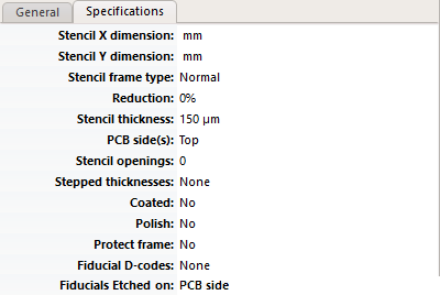 Specifications (Solder paste stencil products)
- Stencil X dimension (mm)
- Stencil Y dimension (mm)
- Stencil frame type: The type of stencil frame pattern. This is usually an extra cost feature if other than Normal.
- Reduction (%): Desired reduction of stencil openings relative to opening size in stencil layer. Normally zero.
- Stencil thickness (µm)
- PCB side(s): The side(s) of the PCB (top|bottom|both) for which the stencil is designed.
- Stencil openings: The number of solder paste openings in the stencil.
- Stepped thicknesses: The number of steps (reduced thicknesses) in the stencil.
- Coated (yes|no): The stencil shall be coated. This is usually an extra cost feature.
- Polish (yes|no): The stencil shall have polished edges on solder paste openings. This is usually an extra cost feature.
- Protect frame (yes|no): The stencil shall be manufactured such that the outer edges are protected from being a cut hazard. This is usually an extra cost feature.
- List of fiducial D-codes: A list of the D-codes in the manufacturing Gerber file which indicate fiducials. Rarely used.
- Fiducials etched on (PCB|Both): Indicates whether fiducials are to be etched on both sides or only the PCB side of the stencil.
Specifications (PCBA products)
- PCB product no.: Macaos product number of PCB product.
- Panel product no.: Macaos product number of panelized PCB product, if any.
- Stencil product no.: Macaos product number of related solder paste stencil product, if any.
- Test fixture product no.: Macaos product number of related test fixture product, if any.
- Depanel fixture product no.: Macaos product number of related depanelization fixture product, if any.
- Solder pallet product no.: Macaos product number of related solder pallet product, if any.
- Top PnP component count: Number of components to be automatically placed on top side.
- Bottom PnP component count: Number of components to be automatically placed on bottom side.
- Non-PnP component count: Number of components to be placed in other processes.
- Total component count: Total number of components.
- Unique component count: Number of unique components.
- BOM data present (yes|no)
- PnP data present (yes|no)
Specifications (Test fixture products)
- Fixture style
- Fixture X dimension (mm)
- Fixture Y dimension (mm)
Specifications (Depanel fixture and Mechanical part products)
- X dimension (mm)
- Y dimension (mm)
- Z dimension (mm)
- Surface area (cm²)
- Volume (cm³)
- Material
- [If depanel fixture] Anti-static (yes|no)
- [If mechanical part] Paint color
Specifications (Solder pallet products)
- Pallet X dimension (mm)
- Pallet Y dimension (mm)
- Pallet material
- Pallet thickness (mm)
- Estimated weight
Specifications (Other product types)
- Items per package
- Weight per package
- [If not connector] Category
- [If connector] Connector style
- Product description
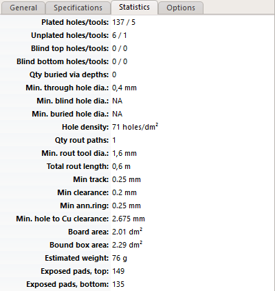 Statistics (PCB products only)
- Plated holes/tools counts
- Unplated holes/tools counts
- Blind top holes/tools counts
- Blind bottom holes/tools counts
- Quantity of buried via depths
- Minimum through hole diameter (mm)
- Minimum blind hole diameter (mm)
- Minimum buried hole diameter (mm)
- Hole density (holes/dm²)
- Rout path count
- Total rout length (mm)
- Minimum track width (mm)
- Minimum clearance (mm)
- Minimum annular ring (mm)
- Minimum hole to copper clearance (mm)
- [If panel] Boards per panel
- [If multi-product panel] Different products per panel
- Board area (dm²)
- Enclosing rectangle area (dm²)
- Estimated weight
- Exposed pad count, top side
- Exposed pad count, bottom side
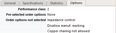 Options (PCB and PCBA products only)
These are order options which are pre-defined for the product. They may be overridden when placing an order.
- Performance class. This is usually an extra cost feature for class 2+ or 3.
- [If PCB product] Impedance control: The manufacturer shall confirm and document that impedance requirements have been met. This is usually an extra cost feature.
- [If PCBA product] Function test of all PCBs: All PCBAs shall be function tested in accordance with customer-supplied test procedure. This is usually an extra cost feature.
- Disallow manufacturer marking: Manufacturer shall not add any identifiers or other markings to the PCB. This option should not be selected if the PCB requires UL marking.
- [If PCB product] Disallow copper shaving: Manufacturer shall not shave (retract) copper away from the board edges or cutouts. This option implies that copper burrs along edges will be accepted. are accepted. This option should only be selected in cases where it is necessary that copper extend to the board edges.
With the exception of Performance class, options which are selected for the product are listed under Pre-selected order options, while the unselected options are listed under Order options not selected.