Import module improvements
Place a text string on the PCB
A text string may be placed on a notation layer of the PCB as follows:
- After linking files and creating an outer contour, click on the Add symbols to board (paintbrush) button, and then click on the Text button.
- Enter the desired text string.
- Select the text height, layer and text rotation, as desired.
- Move the mouse cursor to the desired position and click to place the text.
Add IPC/JEDEC J-STD-609A compliant marking to the PCB
The IPC/JEDEC J-STD-609A stanard defines how PCBs should be marked to identify the the presence (or absence) of lead and/or other attributes in a PCB or PCB assembly. The import module includes a simple dialog box where you can create a compliant text string and add it to a PCB by answering up to 6 questions about the laminate material, surface finish and (optionally) the required assembly processes. Once the text string has been generated, it may be placed at any location on the notation layer of the PCB.
While in Add text mode, click on the J-STD-609A button to open the dialog box. Select the appropriate parameters for the text string, and then click OK. Place the text string as described above.
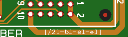
Add remarks to the PCB graphically
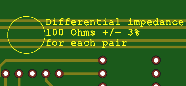
You can add remarks to a PCB at a specific location. This is useful when a remark is tied to some feature or location of the PCB. A remark may be created as follows:
- After linking files and creating an outer contour, click on the Add remarks to board (yellow note) button.
- Draw a circle around the feature(s) to which the remark applies.
- Enter the remark text in the dialog box.
- Click OK.
Remarks are added to the Remarks layer. A circle will be drawn around the selected feature(s) and the remark text placed to the right of the circle.
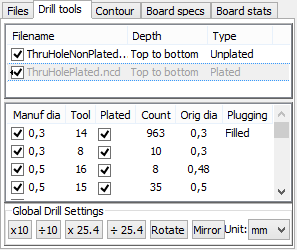 Via protection (plugging, filling, etc)
All holes with a specific drill tool may be specified for via protection. To do this, right-click on the tool in the tool list (of the Drill tools tab) and choose the desired via protection type from the Via protection submenu. A new layer will be created indicating the via holes to be protected.
Create contour segments graphically
When defining an outer or inner contour, the contour must be defined as a closed polygon. If there are missing segments, these can by drawn. This may be done as follows:
- Click on the Draw contour segment (pencil) button.
- Move the cursor to the position where the segment will start. If desired, press the X key to snap the cursor to the nearest existing segment endpoint.
- Click to start the drawn segment.
- Move the cursor to the position where the segment will end. If desired, press the X key to snap the cursor to the nearest existing segment endpoint.
- Click to create the segment.
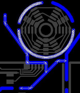
View endpoints of highlighted segments when creating contour
When selecting segments for a contour, the Show endpoints of highlighted segments causes the highlighted segments to be drawn with thin lines and arrowheads. This is useful when trying to see where a gap or overlap exists that prevents the selected segments from being recognized as a closed polygon.
Minimum features
Minimum track width and minimum annular ring are estimated by performing a simple analysis of the imported copper and drill layer data. Minimum clearance is estimated to be the same as the minimum track width. These estimates will be correct in most cases, but some CAD systems generate their trace and/or pad data in a manner that is too complex and time-consuming for the rapid analysis performed by the Import module.
If you know that one or more of the estimated values are incorrect, you should enter the correct values as necessary.
Import of ODB++ jobs
The import module now includes limited support for importing PCB jobs in ODB++ format. An ODB++ job may be imported as a .zip, .gzip, .tgz or .tar archive. When opening an ODB++ project, the layers, outer contour and drill tools are automatically imported and linked. The layers in from the ODB++ project are listed in the ODB++ Layers tab.
If a layer has been linked incorrectly, right-click to link it to a different layer. If the board has inner contours, track routing or scoring, then these must be specified in the normal manner. The stackup, finish and mask colors must also be specified.
If the ODB++ project contains multiple steps, you must choose which step to open. In most cases, one step will be the board and another step will be a panel containing the board. If you are unsure which step to open, choose any step. After viewing the step, you can reopen the file to view a different step, if necessary. The import module has some limitations when working with panelized steps, so we recommend importing the board step and using the Panelization module to create your panel.
Note: Import of ODB++ files is a new technology in the Import module. It has not yet been widely tested by Macaos. Please inspect your board carefully before publishing. If you encounter problems, you can help us improve the ODB++ engine by using the Help|Send problem report command to send us your files together with a description of the problem.
Import of HPGL files
The Import Module has limited support for plotter files in HP-GL format. HP-GL files may be included in a product for documentation purposes only.
Due to the nature of the HP-GL format it is not possible to reliably detect an HP-GL file without parsing the entire file. Therefore, the Import Module detects HP-GL files as Text (or Other, if the file contains plotter setup escape sequences).
To view an HP-GL file, right-click on the file name and choose Change file type|HP-GL. The file will be displayed in the viewer. To include the file in a product, link the file to a User layer. It is not possible to link an HP-GL file to any other layer.
Align pick and place files with Gerber data
If the coordinate origin of pick and place data is different from that of the Gerber data, the offset can be aligned in the same manner as when aligning drill data with Gerber data.
Panelization improvements
Flip board in panel
An individual board in a panel may be flipped upside-down. When a board is flipped, it is mirrored and all of its layers are swapped from top to bottom (and vice versa). This is useful when creating a panel where it is desirable to use the same solder paste stencil for both sides of the panel, or when necessary to improve the copper balance of the panel.
To flip a board, press Shift+Space while the mouse cursor is above the board to be flipped. (The board does not need to be selected.
Clear zone for fiducials
The clear zone around a fiducial mark may be specified as the diameter or width of a circle or square (depending on the soldermask shape). When copper fill is selected for outer layers, then the copper fill will be removed from the clear zone of each fiducial.
Pull scoring line back from panel edges
Scoring lines extend normally from one edge of a panel to the opposite edge. Individual scoring lines may be pulled back from the outside panel edge to the inside edge of the panel frame by holding the mouse cursor over the end of the scoring line and pressing Ctrl+V. Note: Manufacturing a panel with this feature requires Jump Scoring. Not all manufacturers are able to deliver panels with Jump Scoring.
Copper fill on inner layers
Copper fill on inner layers is now generated as a pattern of 5mm diameter dots rather than as solid copper..
Product number layer for multi-product panels
When working with multi-product panels, an additional Product number layer shows the placement and product number of each board in the panel. This layer is for documentation purposes only and may not be exported as a manufacturing layer.
Stencil improvements
Define reduced thickness region based on objects from any layer
When defining a reduced thickness region based on selected objects, the objects may be selected from any layer. The reduced thickness region may either be a rectangle surrounding the selected objects, or may follow the shape(s) of the selected objects plus an "oversize" dimension.
Viewer improvements
View from below
Press the M key to toggle the view between view from above and view from below. When viewed from below, the board is mirrored and only the bottom side layers are visible. This is useful if you wish to see what the bottom side of the product will look like.
Rotate view
Press the R key to toggle the view between unrotated and rotated by 90 degrees. This is useful when viewing a tall, narrow board to make it fit better into the available screen space.
Screen dump
Press Ctrl+V to copy the product viewer image to the clipboard. Press Ctrl+Shift+V to save the product viewer image as a file in PNG (Portable Network Graphics) format.